HOME > GaN Gallium nitride
GaN Gallium nitride
GaN(窒化ガリウム、ガリウムナイトライド)は、シリコンに比べて、バンドギャップが約3倍(3.42eV)広く、絶縁破壊電圧も約10倍(3.0MV/cm)という特性を持っており、Siと同じ10mΩ・cm2までオン抵抗を下げた時、耐圧は1600Vに達します。
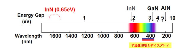
また、青色や緑色といった比較的短い波長の光を発生でき、各種光デバイスにも使用され、SiCと共に次世代パワー半導体デバイスとしても期待されています。
SiCとの比較では、熱伝導率がSiCの方が約3倍高く、それ以外の物性データ(バンドギャップ、電子移動度、絶縁破壊電圧、飽和ドリフト速度)は全てGaNの方が10%程度勝っております。
よって、高温動作環境では、SiCに分が有りますが、電力変換容量、動作周波数の高い領域での使用におきましては、GaNの方が有利と言えます。
The band gap of GaN (Gallium nitride) is wider approximately 3 times (3.42eV) than silicon,
the breakdown voltage has a characteristic of approximately 10 times (3.0MV/cm) in comparison with that.
When I lowered the on-resistance to 10mΩ cm2 same as Si, the withstand voltage of that reaches 1,600V.
In addition, I can generate the light of a relatively short wavelength such as blue and the green and am used in various optodevices,
and GaN (Gallium nitride) is expected as a power semiconductor device with SiC in the next generation.
The thermal conductivity of SiC(Silicon carbide) is higher approximately 3 times than GaN (Gallium nitride),
but at the data of physical property (Bband gap, Electronic mobility, Breakdown voltage, Saturated drift velocity) except it,
GaN is all superior than SiC around 10%.
Thus, in the high temperature environment, SiC has the advantage, but it may be said that GaN is an advantage
when I put it for power conversion capacity, the use in a high operating frequency.
GaNウェハー仕様 GaN Wafer Specification
**画面より大きな表はスクロール可能です
GaN 自立基板 Free-Standing GaN Substrates
| Grade | Production(A-grade) | Research(B-grade) | Dummy(C-grade) |
|---|---|---|---|
| Diamater | Φ2inch | ||
| Thickness | 350,400±30μm | ||
| Surface roughness (Ra) | Ga face:≦0.3nm (Epi-polised) | ||
| N face : 0.5-1.5μm , <0.2nm(Option) | |||
| Orientation | C-plane(0001) off angle toward M , A-axis | ||
| Resistivity(300K) | N-type Undoped:<0.5Ω・cm | ||
| N-type Si-doped:<0.05Ω・cm | |||
| Semi-insulating Fe-doped:1×10⁶Ω・cm | |||
| Usable area | >90% | >80% | >70% |
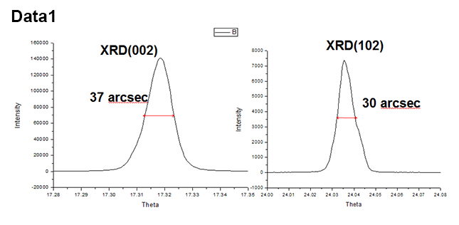
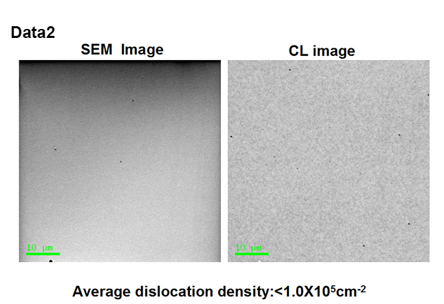
| Dislocation Density | <9.9×105cm-2 | <3×106cm-2 | |
GaN Templates
- GaN on Sapphire(up to 6inch)
- GaN on Si(up to 8inch)
- GaN on SiC(up to 6inch)
- GaN on GaN
| Substrate structure | GaN on Sapphire(0001) | |
|---|---|---|
| Diameter(inch) | 2,4,6 | |
| Epi layerThickness(μm) | 4.5±0.5 , Customized | |
| Conduction Type | N-type(Undoped,Si-doped) P-type(Mg-doped) | |
| Resistivity(300K) | <0.5Ω・cm | |
| Dislocation Density | <5×108cm-2 | |
| Usable Surface Area | >90% | |
| Substrate structure | GaN on Si | |
|---|---|---|
| Diameter(inch) | 4,6,8 | |
| Epi layerThickness(μm) | 4.5±0.5 , Customized | |
| Surface | RMS:<0.5nm in 5X5μm2 | |
| Barrier | AlGaN or AlN or InAlN | |
| Cap layer | In-situ SiN or GaN | |
AlN Tempates
| Substrate structure | AlN on Sapphire , SiC , GaN | |
|---|---|---|
| Diameter(inch) | 2 | |
| Epi layerThickness(nm) | 10~5000(±10%) | |
| Orientation | C-plane(0001)±1° | |
| Conduction Type | Semi-insulating | |
| Dislocation Density | XRD FWHM of (0002) <500arcsec | |
| XRD FWHM of (10-12) <1500arcsec | ||
| Usable Surface Area | >80% | |